2 minute read
 New chip architecture promises a 100x speed boost over GPUs in AI routines
Intel has spent three years developing the new Nervana Neural Network Processor and says that it will accelerate deep learning training models by an impressive degree.
It is probably fair to say that the surge of interest in all things AI caught Intel on the hop, but it came out swinging with an AI roadmap last year that promised to deliver a 100x reduction in the time taken to train a deep learning model by 2020 compared to GPU techniques.
The Nervana Neural Network Processor (NNP) silicon is an important step for the company. While it reckons it powers around 97% of data centre servers running AI workloads, it has been seen to be losing out to GPU-based solutions. Indeed, demand for GPUs from the likes of Nvidia and ARM has gone through the roof in recent times, while Google has been producing its own silicon for its own data centre purposes and now has the second-gen of its own Tensor Processing Unit in its armoury.
The original, said Google, delivered 15–30x higher performance and 30–80x higher performance-per-watt than contemporary CPUs and GPUs. Intel is as yet not commenting on actual performance specs, just saying that it is on track to exceed its 100x promise by 2020 and that it has multiple generations of the technology in the pipeline.
We’ll know more about that claim soon as it is planning on shipping its first NNP silicon to data centres by the end of the year.
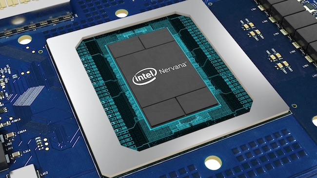
The slightly annoying Nervana name, a rebadge of the silicon formerly codenamed Lake Crest, comes from deep learning startup Nervana Systems, which Intel gobbled up last summer for a rumoured $408 million.
Whatever the name, it’s billed as a purpose-built architecture for the increased computational needs of deep learning. Possibly the main difference between it and previous chip designs is the jettisoning of the standard cache hierarchy and the direct software management of on-chip memory. This improved memory management enables the chip to achieve the higher levels of utilisation of compute on each die necessary for that 100x leap in deep learning training time, while a new numeric format called Flexpoint also promises increased throughput.
According to Intel, this allows scalar computations to be implemented as fixed-point multiplications and additions, while also allowing for large dynamic range using a shared exponent. The upshot of this is, that since each circuit is smaller, this results in a vast increase in parallelism on a die while simultaneously decreasing power per computation.High speed on- and off-chip interconnects meanwhile speed up bi-directional data transfer, with Intel’s stated design goal being to achieve true model parallelism, allowing multiple chips to act as one big virtual one.
The innovation doesn’t end there either, with the company also saying that it is investing in several frontier technologies that will be needed for large-scale computing applications of the future.
Quantum computers are a known quantity in concept, but the delivery last week of a 17-qubit superconducting test chip to Intel’s research partner in the Netherlands, QuTech, marks an important stepping stone inn making them a reality. Even more so when you consider that Intel aims to deliver a 49-qubit chip by the end of this year.
It is also talking about neuromorphic chips, chips that will help computers make decisions based on patterns and associations. These self-learning chips uses data to learn and make inferences, meaning that they don’t need to be trained in the traditional way. Watch below to see more about the first of them, codenamed Loihi.
Tags: Technology

RedShark 2020 @ All rights reserved.

Comments