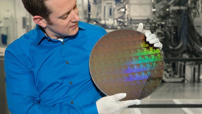
 IBM's Nicolas Loubert holds a wafer of the new 5nm chips
If IBM’s new fabrication process are anything to go by, it looks like the next stages of chip development will be aiming at battery performance in mobile devices rather than out and out grunt.
The recent headlines about IBM’s new fabrication process major on the 5nm die shrink and a continuation of Moore’s (yawn) Law. I’m sorry but I dropped off for a moment there, and with good reason. Moore’s Law is a piece of mythology that has been misused and repurposed over the years by Intel to map out a steady progression in processor technology by claiming that smaller transistors result in a doubling of performance every 18 months or two years
In fact if you look inside a Core i7 you will find a massive part of the die is taken up by cache memory and a significant part is the graphics core. The pipelines of the processor are relatively tiny, and that is where you get the guts of the performance.
By contrast the new 5nm chips from IBM, produced in association with Samsung and GlobalFoundries aren’t so much to do with performance but instead major on efficiency, power and battery life. Let’s face it, when Moore’s Law was coined in 1965, no-one was giving much thought to battery powered smartphones with eight-core processors, 4K displays and high end cameras (plural).
So Nicolas Loubet of IBM was proudly displaying a wafer of 5nm chips, and while the number of nanometres in the fabrication process is only part of the story, it certainly deserves attention. At present Nvidia uses a 16nm process for its mighty GTX graphics chips, Intel and AMD use 14nm in their CPUs and the current Snapdragon 835 from Samsung uses 10nm. The next step after 10nm is 7nm and then 5nm, so IBM is working two steps ahead of the curve.
Using the IBM metric of ‘a chip the size of a fingernail’ (say 12mm x12mm or 150mm2) the previous IBM 7nm process could accommodate 20 billion transistors while the new 5nm process can pack 30 billion transistors in the same area. Snapdragon 835 has a die area around 150 mm^2 and around 3 billion transistors so it is clear that 7nm and then 5nm could result in a massive increase in transistor count or a significant reduction in die area.
I know what you’re thinking; it seems daft that Intel, AMD, Nvidia, Qualcomm, Samsung et al have messed around with 20nm, 14nm, 10nm and 7nm when the obvious thing is to make one massive leap to 5nm and save a lot of time and a huge amount of investment. Well yes, if only life were so simple.
Each die shrink often involves a new fabrication process, new materials and a new chip design. Indeed as far as I can see the only constant in recent generations is that the wafers have remained at 300mm diameter as 400mm appears to be impossible (or uneconomic or unworkable).
Everything else has changed.
To make the 5nm process possible, the IBM Research Alliance with Samsung and GlobalFoundries has made the first use of EUV (Extreme Ultra Violet) lithography. The wavelength of visible light is 400-700nm and clearly useless when you are working at 5nm.
Those 14nm transistors used by Intel and AMD are called Tri-Gate or FinFET (Fin Field Effect Transistor) as they work in three dimensions and derive their name because they are formed with vertical fins. The new 5nm process uses a completely different transistor called Horizontal GAAFET (Gate All Around) which is similar to a FinFET laid down horizontally and wrapped around all four sides of a wire. These sheets are then stacked vertically three-high to achieve greater density. We have seen claims that GAAFET may also work at 3nm.
So yes, IBM has developed the world’s first 5nm chip but there is a great deal more to the story than that, and all we need now is to see 7nm and then 5nm used in a commercial application.
Tags: Technology


Comments